


Financial News
The Glass Age: How Intel’s Breakthrough in Substrates is Rewriting the Rules of AI Compute
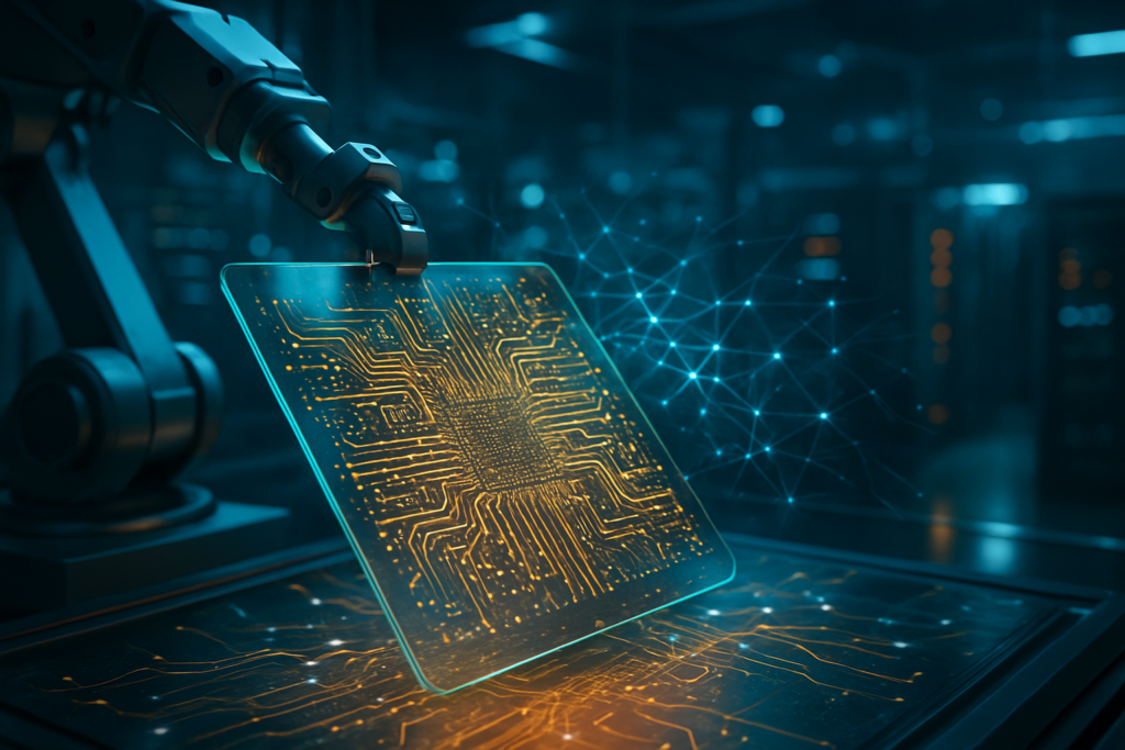
The semiconductor industry has officially entered a new epoch. As of January 2026, the long-predicted "Glass Age" of chip packaging is no longer a roadmap item—it is a production reality. Intel Corporation (NASDAQ: INTC) has successfully transitioned its glass substrate technology from the laboratory to high-volume manufacturing, marking the most significant shift in chip architecture since the introduction of FinFET transistors. By moving away from traditional organic materials, Intel is effectively shattering the "warpage wall" that has threatened to stall the progress of trillion-parameter AI models.
The immediate significance of this development cannot be overstated. As AI clusters scale to unprecedented sizes, the physical limitations of organic substrates—the "floors" upon which chips sit—have become a primary bottleneck. Traditional organic materials like Ajinomoto Build-up Film (ABF) are prone to bending and expanding under the extreme heat generated by modern AI accelerators. Intel’s pivot to glass provides a structurally rigid, thermally stable foundation that allows for larger, more complex "super-packages," enabling the density and power efficiency required for the next generation of generative AI.
Technical Specifications and the Breakthrough
Intel’s technical achievement centers on a high-performance glass core that replaces the traditional resin-based laminate. At the 2026 NEPCON Japan conference, Intel showcased its latest "10-2-10" architecture: a 78×77 mm glass core featuring ten redistribution layers on both the top and bottom. Unlike organic substrates, which can warp by more than 50 micrometers at large sizes, Intel’s glass panels remain ultra-flat, with less than 20 micrometers of deviation across a 100mm surface. This flatness is critical for maintaining the integrity of the tens of thousands of microscopic solder bumps that connect the processor to the substrate.
A key technical differentiator is the use of Through-Glass Vias (TGVs) created via Laser-Induced Deep Etching (LIDE). This process allows for an interconnect density nearly ten times higher than what is possible with mechanical drilling in organic materials. Intel has achieved a "bump pitch" (the distance between connections) as small as 45 micrometers, supporting over 50,000 I/O connections per package. Furthermore, glass boasts a Coefficient of Thermal Expansion (CTE) that nearly matches silicon. This means that as a chip heats up to its peak power—often exceeding 1,000 watts in AI applications—the silicon and the glass expand at the same rate, reducing thermomechanical strain on internal joints by 50% compared to previous standards.
Initial reactions from the semiconductor research community have been overwhelmingly positive, with analysts noting that glass substrates solve the "signal loss" problem that plagued high-frequency 2025-era chips. Glass offers a 60% lower dielectric loss, which translates to a 40% improvement in signal speeds. This capability is vital for the 1.6T networking standards and the ultra-fast data transfer rates required by the latest HBM4 (High Bandwidth Memory) stacks.
Competitive Implications and Market Positioning
The shift to glass substrates creates a new competitive theater for the world's leading chipmakers. Intel has secured a significant first-mover advantage, currently shipping its Xeon 6+ "Clearwater Forest" processors—the first high-volume products to utilize a glass core. By investing over $1 billion in its Chandler, Arizona facility, Intel is positioning itself as the premier foundry for companies like NVIDIA Corporation (NASDAQ: NVDA) and Apple Inc. (NASDAQ: AAPL), who are reportedly in negotiations to secure glass substrate capacity for their 2027 product cycles.
However, the competition is accelerating. Samsung Electronics (KRX:005930) has mobilized a "Triple Alliance" between its display, foundry, and memory divisions to challenge Intel's lead. Samsung is currently running pilot lines in Korea and expects to reach mass production by late 2026. Meanwhile, Taiwan Semiconductor Manufacturing Company (NYSE: TSM) is taking a more measured approach with its CoPoS (Chip-on-Panel-on-Substrate) platform, focusing on refining the technology for its primary client, NVIDIA, with a target of 2028 for full-scale integration.
For startups and specialized AI labs, this development is a double-edged sword. While glass substrates enable more powerful custom ASICs, the high cost of entry for advanced packaging could further consolidate power among "hyperscalers" like Google and Amazon, who have the capital to design their own glass-based silicon. Conversely, companies like Advanced Micro Devices, Inc. (NASDAQ: AMD) are already benefiting from the diversified supply chain; through its partnership with Absolics—a subsidiary of SKC—AMD is sampling glass-based AI accelerators to rival NVIDIA's dominant Blackwell architecture.
Wider Significance for the AI Landscape
Beyond the technical specifications, the emergence of glass substrates fits into a broader trend of "System-on-Package" (SoP) design. As the industry hits the "Power Wall"—where chips require more energy than can be efficiently cooled or delivered—packaging has become the new frontier of innovation. Glass acts as an ideal bridge to Co-Packaged Optics (CPO), where light replaces electricity for data transfer. Because glass is transparent and thermally stable, it allows optical engines to be integrated directly onto the substrate, a feat that Broadcom Inc. (NASDAQ: AVGO) and others are currently exploiting to reduce networking power consumption by up to 70%.
This milestone echoes previous industry breakthroughs like the transition to 193nm lithography or the introduction of High-K Metal Gate technology. It represents a fundamental change in the materials science governing computing. However, the transition is not without concerns. The fragility of glass during the manufacturing process remains a challenge, and the industry must develop new handling protocols to prevent "shattering" events on the production line. Additionally, the environmental impact of new glass-etching chemicals is under scrutiny by global regulatory bodies.
Comparatively, this shift is as significant as the move from vacuum tubes to transistors in terms of how we think about "packaging" intelligence. In the 2024–2025 era, the focus was on how many transistors could fit on a die; in 2026, the focus has shifted to how many dies can be reliably connected on a single, massive glass substrate.
Future Developments and Long-Term Applications
Looking ahead, the next 24 months will likely see the integration of HBM4 directly onto glass substrates, creating "reticle-busting" packages that exceed 100mm x 100mm. These massive units will essentially function as monolithic computers, capable of housing an entire trillion-parameter model's inference engine on a single piece of glass. Experts predict that by 2028, glass substrates will be the standard for all high-end data center hardware, eventually trickling down to consumer devices as AI-driven "personal agents" require more local processing power.
The primary challenge remaining is yield optimization. While Intel has reported steady improvements, the complexity of drilling millions of TGVs without compromising the structural integrity of the glass is a feat of engineering that requires constant refinement. We should also expect to see new hybrid materials—combining the flexibility of organic layers with the rigidity of glass—emerging as "mid-tier" solutions for the broader market.
Conclusion: A Clear Vision for the Future
In summary, Intel’s successful commercialization of glass substrates marks the end of the "Organic Era" for high-performance computing. This development provides the necessary thermal and structural foundation to keep Moore’s Law alive, even as the physical limits of silicon are tested. The ability to match the thermal expansion of silicon while providing a tenfold increase in interconnect density ensures that the AI revolution will not be throttled by the limitations of its own housing.
The significance of this development in AI history will likely be viewed as the moment when the "hardware bottleneck" was finally cracked. While the coming weeks will likely bring more announcements from Samsung and TSMC as they attempt to catch up, the long-term impact is clear: the future of AI is transparent, rigid, and made of glass. Watch for the first performance benchmarks of the Clearwater Forest Xeon chips in late Q1 2026, as they will serve as the first true test of this technology's real-world impact.
This content is intended for informational purposes only and represents analysis of current AI developments.
TokenRing AI delivers enterprise-grade solutions for multi-agent AI workflow orchestration, AI-powered development tools, and seamless remote collaboration platforms.
For more information, visit https://www.tokenring.ai/.
More News
View More


Recent Quotes
View MoreQuotes delayed at least 20 minutes.
By accessing this page, you agree to the Privacy Policy and Terms Of Service.